Early aircraft were equipped with radio communication and navigational devices that were constructed with analog electronic circuits. They used vacuum tubes that functioned as electron control valves. These were later replaced by solid-state devices. Today, digital electronic circuits dominate modern avionics. A brief look at various electron control valves used on aircraft follows.
Electron Control Valves
Electron control valves are an essential part of an electronic circuit. Control of electron flow enables the circuit to produce the desired outcome. Early aircraft made use of vacuum tubes to control electron flow. Later, transistors replaced vacuum tubes. Semiconductors used in transistors and integrated circuits have enabled the solid-state digital electronics found in aircraft today.
Vacuum Tubes
Electron control valves found in the analog circuits of early aircraft electronics are constructed of vacuum tubes. Only antique aircraft retain radios with these devices due to their size and inability to withstand the harsh vibration and shock of the aircraft operating environment. However, they do function, and a description is included here as a foundation for the study of more modern electronic circuits and components.
Diodes
A diode acts as a check valve in an alternating current (AC) circuit. It allows current to flow during half of the AC cycle but not the other half. In this manner, it creates a pulsating direct current (DC) with current that drops to zero in between pulses. A diode tube has two active electrodes: the cathode and the plate. It also contains a heater. All of this is housed in a vacuum environment inside the tube. [Figure 1]
 |
| Figure 1. A vacuum tube diode contains a cathode, heater, and plate. Note that the arrow formed in the symbol for the heater points to the direction of electron flow |
The heater glows red hot while heating the cathode. The cathode is coated with a material whose electrons are excited by the heat. The excited electrons expand their orbit when heated. They move close enough to the plate, which is constructed around the cathode and heater arrangement, that they are attracted to the positively-charged plate.
When the AC current cycles, the plate becomes negatively charged and the excited cathode electrons do not flow to the plate. In a circuit, this causes a check valve effect that allows current to flow only in one direction, which is the definition of a diode. [Figure 2] The various symbols used to depict diodes are shown in Figure 3.
 |
| Figure 2. A vacuum tube diode in a circuit allows current to flow in one direction only. The output waveform illustrates the lack of current flow as the AC cycles |
 |
| Figure 3. Diode symbols |
Triodes
A triode is an electron control valve containing three elements. It is often used to control a large amount of current with a smaller current flow. In addition to the cathode, plate, and heater present in the diode, a triode also contains a grid. The grid is composed of fine wire spiraled between the cathode and the plate but closer to the cathode.
Applying voltage to the grid can influence the cathode’s electrons, which normally flow to the plate when the cathode is heated. Changes in the relatively small amount of current that flows through the grid can greatly impact the flow of electrons from the cathode to the plate. [Figure 4]
 |
| Figure 4. A triode has three elements: the cathode, plate, and a grid |
Figure 5 illustrates a triode in a simple circuit. AC voltage input is applied to the grid. A high-resistance resistor is used so that only a small amount of current passes to the grid. As this small AC input voltage varies, the amount of DC output in the cathode-plate circuit also varies.
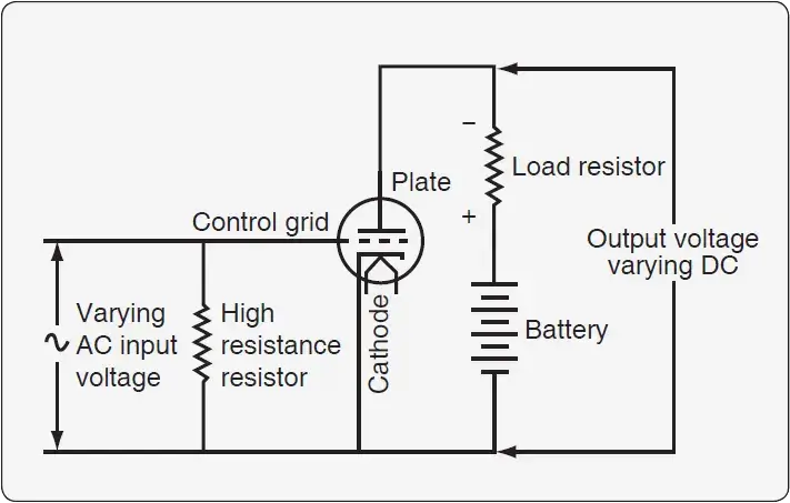 |
| Figure 5. Varying AC input voltage to the grid circuit in a triode produces a varying DC output |
When the input signal is positive, the grid is positive. This aids in drawing electrons from the cathode to the plate. However, when the AC input signal cycles to negative, the grid becomes negatively charged and flow from the cathode to the plate is cut off with the help of the negatively charged grid that repels the electrons on the cathode.
Tetrodes
A tetrode vacuum tube electron control valve has four elements. In addition to the cathode, plate, and grid found in a triode, a tetrode also contains a screen grid. The cathode and plate of a vacuum tube electron control valve can act as a capacitor. At high frequencies, the capacitance is so low that feedback occurs.
The output in the plate circuit feeds back into the control grid circuit. This causes an oscillation generating AC voltage that is unwanted. By placing a screen grid between the anode and the control grid, this feedback and the inter-electrode capacitive effect of the plate and cathode are neutralized. [Figure 6]
 |
| Figure 6. A tetrode is a four element electron control valve vacuum tube including a cathode, a plate, a control grid, and a screen grid |
Figure 7 illustrates a tetrode in a circuit. The screen grid is powered by positive DC voltage. The inter-electrode capacitance is now between the screen grid and the plate. A capacitor is located between the screen grid and ground. AC feedback generated in the screen grid goes to ground and does not oscillate. This allows use of the tetrode at higher frequencies than a triode.
 |
| Figure 7. To enable a triode to be used at high frequencies, a screen grid is constructed between the plate and the control grid |
Pentodes
The plate in a vacuum tube can have a secondary emission that must be controlled. When electrons flow from the cathode through the control grid and screen grid to the plate, they can arrive at such high velocity that some bounce off. Therefore, the tendency is for those electrons to be attracted to the positively charged screen grid. The screen grid is not capable of handling large amounts of current without overheating.
To solve this problem, a third grid is constructed between the plate and the screen grid. Called a suppression grid, it is charged negatively so that secondary electron flow from the plate is repelled by the negative charge back toward the plate and is not allowed to reach the screen grid. The five-element pentode is especially useful in high-power circuits where secondary emissions from the plate are high. [Figure 8]
 |
| Figure 8. A pentode contains a suppression grid that controls secondary electron emissions from the plate at high power. This keeps the current in the screen grid from becoming too high |
Solid-State Devices
Solid-state devices began replacing vacuum tube electron control valves in the late 1950s. Their long life, reliability, and resilience in harsh environments make them ideal for use in avionics.
Semiconductors
The key to solid-state electronic devices is the electrical behavior of semiconductors. To understand semiconductors, a review of what makes a material an insulator or a conductor follows. Then, an explanation for how materials of limited conductivity are constructed and some of their many uses is explained. Semiconductor devices are the building blocks of modern electronics and avionics.
An atom of any material has a characteristic number of electrons orbiting the nucleus of the atom. The arrangement of the electrons occurs in somewhat orderly orbits called rings or shells. The closest shell to the nucleus can only contain two electrons. If the atom has more than two electrons, they are found in the next orbital shell away from the nucleus.
This second shell can only hold eight electrons. If the atom has more than eight electrons, they orbit in a third shell farther out from the nucleus. This third shell is filled with eight electrons and then a fourth shell starts to fill if the element still has more electrons. However, when the fourth shell contains eight electrons, the number of electrons in the third shell begins to increase again until a maximum of 18 is reached. [Figure 9]
 |
| Figure 9. Maximum number of electrons in each orbital shell of an atom |
The outermost orbital shell of any atom’s electrons is called the valence shell. The number of electrons in the valence shell determines the chemical properties of the material. When the valence shell has the maximum number of electrons, it is complete, and the electrons tend to be bound strongly to the nucleus.
Materials with this characteristic are chemically stable. It takes a large amount of force to move the electrons in this situation from one atom valence shell to that of another. Since the movement of electrons is called electric current, substances with complete valence shells are known as good insulators because they resist the flow of electrons (electricity). [Figure 10]
 |
| Figure 10. Elements with full valence shells are good insulators. Most insulators used in aviation are compounds of two or more elements that share electrons to fill their valence shells |
In atoms with an incomplete valence shell, that is, those without the maximum number of electrons in their valence shell, the electrons are bound less strongly to the nucleus. The material is chemically disposed to combine with other materials or other identical atoms to fill in the unstable valence configuration and bring the number of electrons in the valence shell to maximum.
Two or more substances may share the electrons in their valence shells and form a covalent bond. A covalent bond is the method by which atoms complete their valence shells by sharing valence electrons with other atoms.
Electrons in incomplete valence shells may also move freely from valence shell to valence shell of different atoms or compounds. In this case, these are known as free electrons. As stated, the movement of electrons is known as electric current or current flow. When electrons move freely from atom to atom or compound to compound, the substance is known as a conductor. [Figure 11]
 |
| Figure 11. The valence shells of elements that are common conductors have one (or three) electrons |
Not all materials are pure elements, that is, substances made up of one kind of atom. Compounds occur when two or more different types of atoms combine. They create a new substance with different characteristics than any of the component elements.
When compounds form, valence shells and their maximum number of electrons remain the rule of physics. The new compound molecule may either share electrons to fill the valence shell or free electrons may exist to make it a good conductor.
Silicon is an atomic element that contains four electrons in its valence shell. It tends to combine readily with itself and form a lattice of silicon atoms in which adjacent atoms share electrons to fill out the valence shell of each to the maximum of eight electrons. [Figure 12] This unique symmetric alignment of silicon atoms results in a crystalline structure.
 |
| Figure 12. The silicon atoms with just the valence shell electrons share these valence electrons with each other. By sharing with four other silicon atoms, the number of electrons in each silicon atom valence shell becomes eight, which is the maximum number. This makes the substance stable and it resists any flow of electrons |
Once bound together, the valence shells of each silicon atom are complete. In this state, movement of electrons does not occur easily. There are no free electrons to move to another atom and no space in the valence shells to accept a free electron. Therefore, silicon in this form is a good insulator.
Silicon is a primary material used in the manufacture of semiconductors. Germanium and a few other materials are also used.
Since silicon is an insulator, it must be modified to become a semiconductor. The process often used is called doping. Starting with ultra-pure silicon crystal, arsenic, phosphorus, or some other element with five valence electrons in each atom is mixed into the silicon. The result is a silicon lattice with flaws. [Figure 13]
 |
| Figure 13. Silicon atoms doped with arsenic form a lattice work of covalent bonds. Free electrons exist in the material from the arsenic atom’s 5th valence electron. These are the electrons that flow when the semiconductor material, known as N-type or donor material, is conducting |
The elements bond, but numerous free electrons are present in the material from the 5th electron that is part of the valence shell of the doping element atoms. These free electrons can now flow under certain conditions. Thus, the silicon becomes semiconductive. The conditions required for electron flow in a semiconductor are discussed in the following paragraphs.
When silicon is doped with an element or compound containing five electrons in its valence shell, the result is a negatively charged material due to the excess free electrons, and the fact that electrons are negatively charged. This is known as an N-type semiconductor material. It is also known as a donor material because, when it is used in electronics, it donates the extra electrons to current flow.
Doping silicon can also be performed with an element that has only three valence electrons, such as boron, gallium, or indium. Valence electron sharing still occurs, and the silicon atoms with interspersed doping element atoms form a lattice molecular structure.
However, in this case, there are many valence shells where there are only seven electrons and not eight. This greatly changes the properties of the material. The absence of the electrons, called holes, encourages electron flow due to the preference to have eight electrons in all valence shells. Therefore, this type of doped silicon is also semiconductive. It is known as P-type material or as an acceptor since it accepts electrons in the holes under certain conditions. [Figure 14]
 |
| Figure 14. The lattice of boron doped silicon contains holes where the three boron valence shell electrons fail to fill in the combined valence shells to the maximum of eight electrons. This is known as P-type semiconductor material or acceptor material |
Combining N- and P-type semiconductor material in certain ways can produce very useful results. A look at various semiconductor devices follows.
Semiconductor Diodes
A diode is an electrical device that allows current to flow in one direction through the device but not the other. A simple device that can be made from N- and P-type semiconductors is a semiconductor diode. When joined, the junction of these two materials exhibits unique properties. Since there are holes in the P-type material, free electrons from the N-type material are attracted to fill these holes. Once combined, the area at the junction of the two materials where this happens is said to be depleted.
There are no longer free electrons or holes. However, having given up some electrons, the N-type material next to the junction becomes slightly positively charged, and having received electrons, the P-type material next to the junction becomes slightly negatively charged.
The depletion area at the junction of the two semiconductor materials constitutes a barrier or potential hill. The intensity of the potential hill is proportional to the width of the depletion area (where the electrons from the N-type material have filled holes in the P-type material). [Figure 15]
 |
| Figure 15. A potential hill |
The two semiconductors joined in this manner form a diode that can be used in an electrical circuit. A voltage source is attached to the diode. When the negative terminal of the battery is attached to the N-type semiconductor material and the positive terminal is attached to the P-type material, electricity can flow in the circuit.
The negative potential of the battery forces free electrons in the N-type material toward the junction. The positive potential of the battery forces holes in the P-type material toward the other side of the junction. The holes move by the rebinding of the doping agent ions closer to the junction. At the junction, free electrons continuously arrive and fill the holes in the lattice.
As this occurs, more room is available for electrons and holes to move into the area. Pushed by the potential of the battery, electrons and holes continue to combine. The depletion area becomes extremely narrow under these conditions. The potential hill or barrier is, therefore, very small. The flow of current in the electrical circuit is in the direction of electron movement shown in Figure 16.
 |
| Figure 16. The flow of current and the P-N junction of a semiconductor diode attached to a battery in a circuit |
In similar circuits where the negative battery terminal is attached to the N-type semiconductor material and the positive terminal is attached to the P-type material, current flows from N-type, or donor material, to P-type acceptor material. This is known as a forward-biased semiconductor.
A voltage of approximately 0.7 volts is needed to begin the current flow over the potential hill. Thereafter, current flow is linear with the voltage. However, temperature affects the ease at which electrons and holes combine given a specific voltage.
If the battery terminals are reversed, the semiconductor diode circuit is said to be reverse biased. [Figure 17]
 |
| Figure 17. A reversed biased condition |
Attaching the negative terminal of the battery to the P-type material attracts the holes in the P-type material away from the junction in the diode. The positive battery terminal attached to the N-type material attracts the free electrons from the junction in the opposite direction.
In this way, the width of the area of depletion at the junction of the two materials increases. The potential hill is greater. Current cannot climb the hill; therefore, no current flows in the circuit. The semiconductors do not conduct.
Semiconductor diodes are used often in electronic circuits. When AC current is applied to a semiconductor diode, current flows during one cycle of the AC but not during the other cycle. The diode, therefore, becomes a rectifier.
When it is forward biased, electrons flow; when the AC cycles, electrons do not flow. A simple AC rectifier circuit containing a semiconductor diode and a load resistor is illustrated in Figure 18. Semiconductor diode symbols and examples of semiconductor diodes are shown in Figure 19.
 |
| Figure 18. A semiconductor diode acts as a check valve in an AC circuit resulting in a pulsating DC output |
 |
| Figure 19. Symbols and drawings of semiconductor diodes |
Semiconductor diodes have limitations. They are rated for a range of current flow. Above a certain level, the diode overheats and burns up. The amount of current that passes through the diode when forward biased is directly proportional to the amount of voltage applied. But, as mentioned, it is affected by temperature.
Figure 20 indicates the actual behavior of a semiconductor diode. In practice, a small amount of current does flow through a semiconductor diode when reversed biased. This is known as leakage current and it is in the microampere range. However, at a certain voltage, the blockage of current flow in a reversed biased diode breaks down completely. This voltage is known as the avalanche voltage because the diode can no longer hold back the current and the diode fails.
 |
| Figure 20. A semiconductor diode |
Zener Diodes
Diodes can be designed with a zener voltage. This is similar to avalanche flow. When reversed biased, only leakage current flows through the diode. However, as the voltage is increased, the zener voltage is reached. The diode lets current flow freely through the diode in the direction in which it is normally blocked. The diode is constructed to be able to handle the zener voltage and the resulting current, whereas avalanche voltage burns out a diode.
A zener diode can be used as means of dropping voltage or voltage regulation. It can be used to step down circuit voltage for a particular application but only when certain input conditions exist. Zener diodes are constructed to handle a wide range of voltages. [Figure 21]
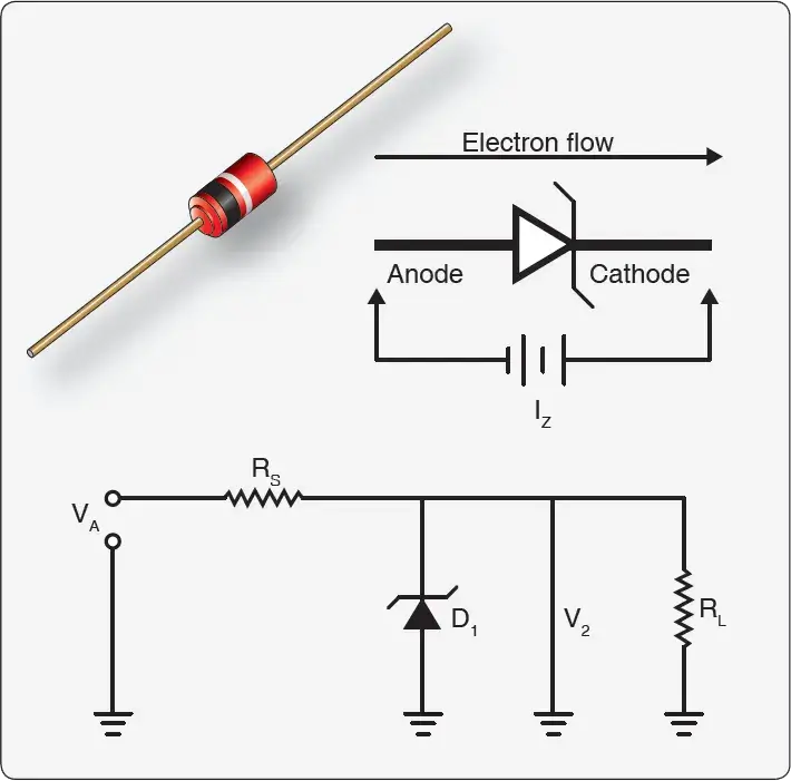 |
| Figure 21. A zener diode, when reversed biased, will break down and allow a prescribed voltage to flow in the direction normally blocked by the diode |
Transistors
While diodes are very useful in electronic circuits, semiconductors can be used to construct true control valves known as transistors. A transistor is little more than a sandwich of N-type semiconductor material between two pieces of P-type semiconductor material or vice versa.
However, a transistor exhibits some remarkable properties and is the building block of modern electronic devices. [Figure 22] As with any union of dissimilar types of semiconductor materials, the junctions of the P- and N- materials in a transistor have depletion areas that create potential hills for the flow of electrical charges.
 |
| Figure 22. Typical transistors, diagrams of a PNP and NPN transistor, and the symbol for those transistors when depicted in an electronic circuit diagram |
Like a vacuum tube triode, the transistor has three electrodes or terminals, one each for the three layers of semiconductor material. The emitter and the collector are on the outside of the sandwiched semiconductor material. The center material is known as the base.
A change in a relatively small amount of voltage applied to the base of the transistor allows a relatively large amount of current to flow from the collector to the emitter. In this way, the transistor acts as a switch with a small input voltage controlling a large amount of current.
If a transistor is put into a simple battery circuit, such as the one shown in Figure 23, voltage from the battery (EB) forces free electrons and holes toward the junction between the base and the emitter just as it does in the junction of a semiconductor diode.
 |
| Figure 23. The effect of applying a small voltage to bias the emitter-base junction of a transistor (top). A circuit diagram for this same transistor (bottom) |
The emitter-base depletion area becomes narrow as free electrons combine with the holes at the junction. Current (IB) (solid arrows) flows through the junction in the emitter-base battery circuit. At the same time, an emitter-collector circuit is constructed with a battery (EC) of much higher voltage in its circuit.
Because of the narrow depletion area at the emitter-base junction, current IC is able to cross the collector base junction, flow through emitter-base junction, and complete the collector-emitter battery circuit (hollow arrows).
To some extent, varying the voltage to the base material can increase or decrease the current flow through the transistor as the emitter-base depletion area changes width in response to the base voltage. If base voltage is removed, the emitter-base depletion area becomes too wide and all current flow through the transistor ceases.
Current in the transistor circuit illustrated has a relationship as follows: IE = IB + IC. It should be remembered that it is the voltage applied to the base that turns the collector-emitter transistor current on or off.
Controlling a large amount of current flow with a small independent input voltage is very useful when building electronic circuits. Transistors are the building blocks from which all electronic devices are made, including Boolean gates that are used to create microprocessor chips.
As production techniques have developed, the size of reliable transistors has shrunk. Now, hundreds of millions and even billions of transistors may be used to construct a single chip such as the one that powers your computer and various avionic devices.
Silicon Controlled Rectifiers
Combination of semiconductor materials is not limited to a two-type, three-layer sandwich transistor. By creating a four-layer sandwich of alternating types of semiconductor material (i.e., PNPN or NPNP), a slightly different semiconductor diode is created. As is the case in a two-layer diode, circuit current is either blocked or permitted to flow through the diode in a single direction.
Within a four-layer diode, sometimes known as a Shockley diode, there are three junctions. The behavior of the junctions and the entire four-layer diode can be understood by considering it to be two interconnected three-layer transistors. [Figure 24]
 |
| Figure 24. A four-layer semiconductor diode behaves like two transistors. When breakover voltage is reached, the device conducts current until the voltage is removed |
Transistor behavior includes no current flow until the base material receives an applied voltage to narrow the depletion area at the base-emitter junction. The base materials in the four-layer diode transistor model receive charge from the other transistor’s collector. With no other means of reducing any of the depletion areas at the junctions, it appears that current does not flow in either direction in this device.
However, if a large voltage is applied to forward bias the anode or cathode, at some point the ability to block flow breaks down. Current flows through whichever transistor is charged. Collector current then charges the base of the other transistor and current flows through the entire device.
Some caveats are necessary with this explanation. The transistors that comprise this four-layer diode must be constructed of material similar to that described in a zener diode. That is, it must be able to endure the current flow without burning out. In this case, the voltage that causes the diode to conduct is known as breakover voltage rather than breakdown voltage.
Additionally, this diode has the unique characteristic of allowing current flow to continue until the applied voltage is reduced significantly, in most cases, until it is reduced to zero. In AC circuits, this would occur when the AC cycles.
While the four-layer, Shockley diode is useful as a switching device, a slight modification to its design creates a silicon-controlled rectifier (SCR). To construct a SCR, an additional terminal known as a gate is added. It provides more control and utility.
In the four-layer semiconductor construction, there are always two junctions forward biased and one junction reversed biased. The added terminal allows the momentary application of voltage to the reversed biased junction. All three junctions then become forward biased and current at the anode flows through the device.
Once voltage is applied to the gate, the SCR becomes latched or locked on. Current continues to flow through it until the level drops off significantly, usually to zero. Then, another applied voltage through the gate is needed to reactivate the current flow. [Figures 25 and 26]
 |
| Figure 25. A silicon controlled rectifier (SCR) allows current to pass in one direction when the gate receives a positive pulse to latch the device in the on position. Current ceases to flow when it drops below holding current, such as when AC current reverses cycle |
 |
| Figure 26. Cross-section of a medium-power SCR |
SCRs are often used in high voltage situations, such as power switching, phase controls, battery chargers, and inverter circuits. They can be used to produce variable DC voltages for motors and are found in welding power supplies.
Often, lighting dimmer systems use SCRs to reduce the average voltage applied to the lights by only allowing current flow during part of the AC cycle. This is controlled by controlling the pulses to the SCR gate and eliminating the massive heat dissipation caused when using resistors to reduce voltage.
Figure 27 graphically depicts the timing of the gate pulse that limits full cycle voltage to the load. By controlling the phase during which the SCR is latched, a reduced average voltage is applied.
 |
| Figure 27. Phase control is a key application for SCR. By limiting the percentage of a full cycle of AC voltage that is applied to a load, a reduced voltage results. The firing angle or timing of a positive voltage pulse through the SCR’s gate latches the device open allowing current flow until it drops below the holding current, which is usually at or near zero voltage as the AC cycle reverses |
Triacs
SCRs are limited to allowing current flow in one direction only. In AC circuitry, this means only half of the voltage cycle can be used and controlled. To access the voltage in the reverse cycle from an AC power source, a triac can be used. A triac is also a four-layer semiconductor device. It differs from an SCR in that it allows current flow in both directions.
A triac has a gate that works the same way as in a SCR; however, a positive or negative pulse to the gate triggers current flow in a triac. The pulse polarity determines the direction of the current flow through the device.
Figure 28 illustrates a triac and shows a triac in a simple circuit. It can be triggered with a pulse of either polarity and remains latched until the voltage declines, such as when the AC cycles.
 |
| Figure 28. A triac is a controlled semiconductor device that allows current flow in both directions |
Then, it needs to be triggered again. In many ways, the triac acts as though it is two SCRs connected side by side only in opposite directions. Like an SCR, the timing of gate pulses determines the amount of the total voltage that is allowed to pass.
The output waveform if triggered at 90° is shown in Figure 28. Because a triac allows current to flow in both directions, the reverse cycle of AC voltage can also be used and controlled.
When used in actual circuits, triacs do not always maintain the same phase firing point in reverse as they do when fired with a positive pulse. This problem can be regulated somewhat through the use of a capacitor and a diac in the gate circuit.
However, as a result, where precise control is required, two SCRs in reverse of each other are often used instead of the triac. Triacs do perform well in lower voltage circuits. Figure 29 illustrates the semiconductor layering in a triac.
 |
| Figure 29. The semiconductor layering in a triac. A positive or negative gate pulse with respect to the upper terminal allows current to flow through the devise in either direction |
Unijunction Transistors (UJT)
The behavior of semiconductor materials is exploited through the construction of numerous transistor devices containing various configurations of N-type and P-type materials. The physical arrangement of the materials in relation to each other yields devices with unique behaviors and applications.
The transistors described above having two junctions of P-type and N-type materials (PN) are known as bipolar junction transistors. Other more simple transistors can be fashioned with only one junction of the PN semiconductor materials. These are known as unijunction transistors (UJT). [Figure 30]
 |
| Figure 30. A unijunction transistor (UJT) |
The UJT contains one base semiconductor material and a different type of emitter semiconductor material. There is no collector material. One electrode is attached to the emitter and two electrodes are attached to the base material at opposite ends.
These are known as base 1 (B1) and base 2 (B2). The electrode configuration makes the UJT appear physically the same as a bipolar junction transistor. However, there is only one PN junction in the UJT and it behaves differently.
The base material of a UJT behaves like a resistor between the electrodes. With B2 positive with respect to B1, voltage gradually drops as it flows through the base. [Figure 31]
 |
| Figure 31. The voltage gradient in a UJT |
By placing the emitter at a precise location along the base material gradient, the amount of voltage needed to be applied to the emitter electrode to forward bias the UJT base-emitter junction is determined. When the applied emitter voltage exceeds the voltage at the gradient point where the emitter is attached, the junction is forward biased and current flows freely from the B1 electrode to the E electrode.
Otherwise, the junction is reverse biased and no significant current flows although there is some leakage. By selecting a UJT with the correct bias level for a particular circuit, the applied emitter voltage can control current flow through the device.
UJTs of a wide variety of designs and characteristics exist. A description of all of them is beyond the scope of this discussion. In general, UJTs have some advantages over bipolar transistors. They are stable in a wide range of temperatures. In some circuits, use of UJTs can reduce the overall number of components used, which saves money and potentially increases reliability.
They can be found in switching circuits, oscillators, and wave shaping circuits. However, four-layered semiconductor thyristors that function the same as the UJT just described are less expensive and most often used.
Field Effect Transistors (FET)
As shown in the triac and the UJT, creative arrangement of semiconductor material types can yield devices with a variety of characteristics. The field effect transistor (FET) is another such device which is commonly used in electronic circuits. Its N- and P-type material configuration is shown in Figure 32.
 |
| Figure 32. The basic structure of a field effect transistor and its electronic symbol |
A FET contains only one junction of the two types of semiconductor material. It is located at the gate where it contacts the main current carrying portion of the device. Because of this, when an FET has a PN junction, it is known as a junction field effect transistor (JFET). All FETs operate by expanding and contracting the depletion area at the junction of the semiconductor materials.
One of the materials in a FET or JFET is called the channel. It is usually the substrate through which the current needing to be controlled flows from a source terminal to a drain terminal. The other type of material intrudes into the channel and acts as the gate. The polarity and amount of voltage applied to the gate can widen or narrow the channel due to expansion or shrinking of the depletion area at the junction of the semiconductors.
This increases or decreases the amount of current that can flow through the channel. Enough reverse-biased voltage can be applied to the gate to prevent the flow of current through the channel. This allows the FET to act as a switch. It can also be used as a voltage-controlled resistance.
FETs are easier to manufacture than bipolar transistors and have the advantage of staying on once current flow begins without continuous gate voltage applied. They have higher impedance than bipolar transistors and operate cooler. This makes their use ideal for integrated circuits where millions of FETs may be in use on the same chip. FETs come in N-channel and P-channel varieties.
Metal Oxide Semiconductor Field Effect Transistors (MOSFETs) and Complementary Metal Oxide Semiconductor (CMOS)
The basic FET has been modified in numerous ways and continues to be at the center of faster and smaller electronic component development. A version of the FET widely used is the metal oxide semiconductor field effect transistor (MOSFET). The MOSFET uses a metal gate with a thin insulating material between the gate and the semiconductor material.
This essentially creates a capacitor at the gate and eliminates current leakage in this area. Modern versions of the MOSFET have a silicon dioxide insulating layer and many have poly-crystalline silicon gates rather than metal, but the MOSFET name remains and the basic behavioral characteristics are the same. [Figure 33]
 |
| Figure 33. A MOSFET has a metal gate and an oxide layer between it and the semiconductor material to prevent current leakage |
As with FETs, MOSFETs come with N-channels or P-channels. They can also be constructed as depletion mode or enhancement mode devices. This is analogous to a switch being normally open or normally closed. Depletion mode MOSFETs have an open channel that is restricted or closed when voltage is applied to the gate (i.e., normally open).
Enhancement mode MOSFETs allow no current to flow at zero bias but create a channel for current flow when voltage is applied to the gate (normally closed). No voltage is used when the MOSFETs are at zero bias. Millions of enhancement mode MOSFETs are used in the construction of integrated circuits. They are installed in complimentary pairs such that when one is open, the other is closed.
This basic design is known as complementary MOSFET (CMOS), which is the basis for integrated circuit design in nearly all modern electronics. Through the use of these transistors, digital logic gates can be formed, and digital circuitry is constructed.
Other more specialized FETs exist. Some of their unique characteristics are owed to design alterations and others to material variations. The transistor devices discussed above use silicon-based semiconductors. But the use of other semiconductor materials can yield variations in performance.
Metal semiconductor FETs (MESFETS) for example, are often used in microwave applications. They have a combined metal and semiconductor material at the gate and are typically made from gallium arsenide or indium phosphide. MESFETs are used for their quickness when starting and stopping current flows especially in opposite directions.
High electron mobility transistors (HEMT) and pseudomorphic high electron mobility transistors (PHEMT) are also constructed from gallium arsenide semiconductor material and are used for high-frequency applications.
Photodiodes and Phototransistors
Light contains electromagnetic energy that is carried by photons. The amount of energy depends on the frequency of light of the photon. This energy can be very useful in the operation of electronic devices since all semiconductors are affected by light energy. When a photon strikes a semiconductor atom, it raises the energy level above what is needed to hold its electrons in orbit.
The extra energy frees an electron enabling it to flow as current. The vacated position of the electron becomes a hole. In photodiodes, this occurs in the depletion area of the reversed biased PN junction turning on the device and allowing current to flow.
Figure 34 illustrates a photodiode in a coil circuit. In this case, the light striking the photodiode causes current to flow in the circuit whereas the diode would have otherwise blocked it. The result is the coil energizes and closes another circuit enabling its operation.
 |
| Figure 34. The symbol for a photodiode and a photodiode in a simple coil circuit |
A photon activated transistor could be used to carry even more current than a photodiode. In this case, the light energy is focused on a collector-base junction. This frees electrons in the depletion area and starts a flow of electrons from the base that turns on the transistor.
Once on, heavier current flows from the emitter to the collector. [Figure 35] In practice, engineers have developed numerous ways to use the energy in light photons to trigger semiconductor devices in electronic circuits. [Figure 36]
 |
| Figure 35. A photo transistor in a simple coil circuit (bottom) and the symbol for a phototransistor (top) |
 |
| Figure 36. Phototransistors |
Light-Emitting Diodes
Light-emitting diodes (LEDs) have become so commonly used in electronics that their importance may tend to be overlooked. Numerous avionics displays and indicators use LEDs for indicator lights, digital readouts, and backlighting of liquid crystal display (LCD) screens.
LEDs are simple and reliable. They are constructed of semiconductor material. When a free electron from a semiconductor drops into a semiconductor hole, energy is given off. This is true in all semiconductor materials.
However, the energy released when this happens in certain materials is in the frequency range of visible light. Figure 37 is a table that illustrates common LED colors and the semiconductor material that is used in the construction of the diode.
 |
| Figure 37. LED colors and the materials used to construct them as well as their wavelength and voltages |
 |
| Figure 38. A close up of a single LED (left) and the process of a semi-conductor producing light by electrons dropping into holes and giving off energy (right). The symbol for a light emitting diode is the diode symbol with two arrows pointing away from the junction |
Why were vacuum tubes replaced by solid-state devices in aviation?
What is the difference between N-type and P-type semiconductor materials?
How does a transistor act as an electron control valve?
What are the advantages of Field Effect Transistors (FETs) in integrated circuits?
RELATED POSTS