The solid-state semiconductor devices described in the previous Electron Control Valves section can be found in both analog and digital electronic circuits. As digital electronics continue to evolve, many analog circuits are being replaced. However, many aircraft still use analog electronics in radio and navigation equipment, as well as in other aircraft systems. A brief overview of some basic analog circuits follows.
Rectifiers
Rectifier circuits change AC voltage into DC voltage and are one of the most commonly used types of circuits in aircraft electronics. [Figure 1]
 |
| Figure 1. A half wave rectifier uses one diode to produce pulsating DC current from AC. Half of the AC cycle is wasted when the diode blocks the current flow as the AC cycles below zero |
The resulting DC waveform output is also shown. The circuit has a single semiconductor diode and a load resistor. When the AC voltage cycles below zero, the diode shuts off and does not allow current flow until the AC cycles through zero voltage again. The result is pronounced pulsating DC. While this can be useful, half of the original AC voltage is not being used.
A full wave rectifier creates pulsating DC from AC while using the full AC cycle. One way to do this is to tap the secondary coil at its midpoint and construct two circuits with the load resistor and a diode in each circuit. [Figure 2] The diodes are arranged so that when current is flowing through one, the other blocks current.
 |
| Figure 2. A full wave rectifier can be built by center tapping the secondary coil of the transformer and using two diodes in separate circuits. This rectifies the entire AC input into a pulsating DC with twice the frequency of a half wave rectifier |
When the AC cycles so the top of the secondary coil of the transformer is positive, current flows from ground, through the load resistor (VRL), Diode 1 (D1), and the upper half of the coil. Current cannot flow through Diode 2 (D2) because it is blocked. [Figure 2A]
As the AC cycles through zero, the polarity of the secondary coil changes. [Figure 2B] Current then flows from ground, through the load resistor, Diode 2 (D2), and the bottom half of the secondary coil. Current flow through Diode 1 (D1) is blocked. This arrangement yields positive DC from alternating AC cycles with no wasted current.
Another way to construct a full wave rectifier uses four semiconductor diodes in a bridge circuit. Because the secondary coil of the transformer is not tapped at the center, the resultant DC voltage output is greater than that of the two-diode full-wave rectifier because the entire secondary winding is utilized. [Figure 3] During the first half of the AC cycle, the bottom of the secondary coil is negative.
 |
| Figure 3. The bridge-type four-diode full wave rectifier circuit is most commonly used to rectify single-phase AC into DC |
Current flows from it through Diode 1 (D1), then through the load resistor, and through Diode 2 (D2) on its way back to the top of the secondary coil. When the AC reverses its cycle, the polarity of the secondary coil changes. Current flows from the top of the coil through Diode 3 (D3), then through the load resistor, and through Diode 4 (D4) on its way back to the bottom of the secondary coil. The output waveform reflects the higher voltage achieved by rectifying the full AC cycle through the entire length of the secondary coil.
Use and rectification of three-phase AC is also possible on aircraft with a specific benefit. The output DC is very smooth and does not drop to zero. A six-diode circuit is built to rectify the typical three-phase AC produced by an aircraft alternator. [Figure 4]
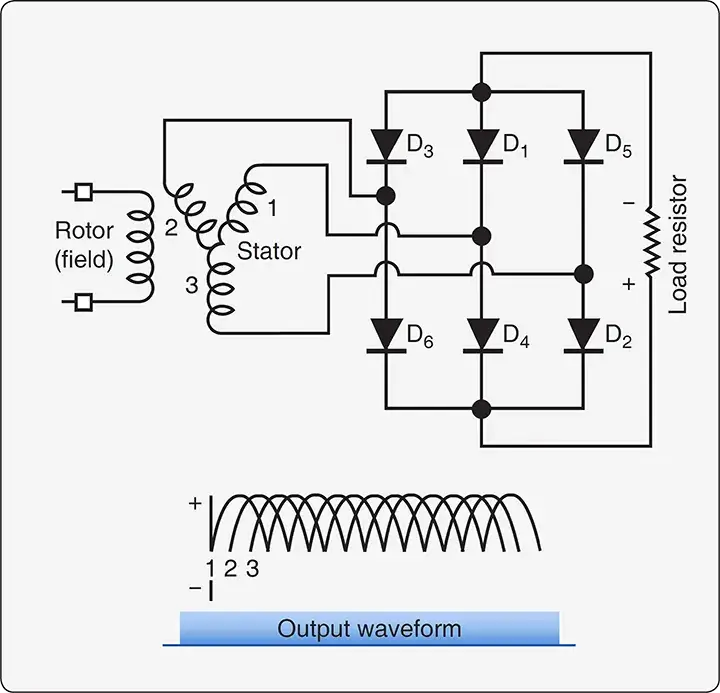 |
| Figure 4. A six-diode, three-phase AC rectifier |
Each stator coil corresponds to a phase of AC and becomes negative for 120° of rotation of the rotor. When stator 1 or the first phase is negative, current flows from it through Diode 1 (D1), then through the load resistor and through Diode 2 (D2) on its way back to the third phase coil.
Next, the second phase coil becomes negative and current flows through Diode 3 (D3). It continues to flow through the load resistor and Diode 4 (D4) on its way back to the first phase coil. Finally, the third phase coil becomes negative causing current to flow through Diode 5 (D5), then the load resistor and Diode 6 (D6) on its way back to the second phase coil.
The output waveform of this three-phase rectifier depicts the DC produced. It is a relatively steady, nearly non-pulsing flow equivalent to just the tops of the individual curves. The phase overlap prevents voltage from falling to zero, producing smooth DC from AC.
Amplifiers
An amplifier is a circuit that changes the amplitude of an electric signal. This is done through the use of transistors. As mentioned, a transistor that is forward biased at the base-emitter junction and reverse biased at the collector-base junction is turned on. It can conduct current from the collector to the emitter. Because a small signal at the base can cause a large current to flow from collector to emitter, a transistor in itself can be said to be an amplifier.
However, a transistor properly wired into a circuit with resistors, power sources, and other electronic components, such as capacitors, can precisely control more than signal amplitude. Phase and impedance can also be manipulated.
Since the typical bipolar junction transistor requires a base circuit and a collector-emitter circuit, there should be four terminals, two for each circuit. However, the transistor only has three terminals (i.e., the base, the collector, and the emitter). Therefore, one of the terminals must be common to both transistor circuits. The selection of the common terminal affects the output of the amplifier.
The three basic amplifier types, named for which terminal of the transistor is the common terminal to both transistor circuits, include:
- Common-emitter amplifier
- Common-collector amplifier
- Common-base amplifier
Common-Emitter Amplifier
The common-emitter amplifier controls the amplitude of an electric signal and inverts the phase of the input signal. Figure 5 illustrates a common-emitter amplifier for AC using a NPN transistor and its output signal graph.
Common emitter circuits are characterized by high current gain and a 180° voltage phase shift from input to output. It can be used to amplify microphone signals to drive a speaker. As always, adequate voltage of the correct polarity to the base puts the transistor in the active mode or turns it on.
Then, as the base input current fluctuates, the current through the transistor fluctuates proportionally. However, AC cycles through positive and negative polarity. Every 180°, the transistor shuts off because the polarity to the base-emitter junction of the transistor is not correct to forward bias the junction.
To keep the transistor on, a DC biasing voltage of the correct polarity (shown as a 2.3-volt battery) is placed in series with the input signal in the base circuit to hold the transistor in the active mode as the AC polarity changes. This way the transistor stays in the active mode to amplify an entire AC signal.
Transistors are rated by ratio of the collector current to the base current, or Beta (β). This is established during the manufacture of the unit and cannot be changed. A transistor with a β value of 100 can handle 100 times more current through a collector-emitter circuit than the base input signal.
This current in Figure 5 is provided from the 15V battery, V1. So, the amplitude of amplification is a factor of the beta of the transistor and any in-line resistors used in the circuits. The fluctuations of the output signal, however, are entirely controlled by the fluctuations of current input to the transistor base.
If measurements of input and output voltages are made, it is shown that as the input voltage increases, the output voltage decreases. This accounts for the inverted phase produced by a common-emitter circuit. [Figure 5]
 |
| Figure 5. A common-emitter amplifier circuit for amplifying an AC microphone signal to drive a speaker (top) and the graph of the output signal showing a 180 degree shift in phase (bottom) |
Common-Collector Amplifier
Another basic type of amplifier circuit is the common-collector amplifier. Common-collector circuits are characterized by high current gain, but virtually no voltage gain. The input circuit and the load circuit in this amplifier share the collector terminal of the transistor used.
Because the load is in series with the emitter, both the input current and output current run through it. This causes a directly proportional relationship between the input and the output. The current gain in this circuit configuration is high. A small amount of input current can control a large amount of current to flow from the collector to the emitter. A common collector amplifier circuit is illustrated in Figure 6.
 |
| Figure 6. A basic common-collector amplifier circuit. Both the input and output circuits share a path through the load and the emitter. This causes a direct relationship of the output current to the input current |
The base current needs to flow through the PN junction of the transistor, which has about a 0.7 V threshold to be turned on. The current gain of the amplifier is approximately the beta value of the transistor plus 1.
During AC amplification, the common-collector amplifier has the same problem that exists in the common-emitter amplifier. The transistor must stay on or in the active mode regardless of input signal polarity. When the AC cycles through zero, the transistor turns off because the minimum amount of current to forward bias the transistor is not available.
The addition of a DC biasing source (battery) in series with the AC signal in the input circuit keeps the transistor in the active mode throughout the full AC cycle. [Figure 7]
 |
| Figure 7. A DC biasing current is used to keep the transistor of a common-collector amplifier in the active mode when amplifying AC (top). The output of this amplifier is in phase and directly proportional to the input (bottom). The difference in amplitude between the two is the 0.7V used to bias the PN junction of the transistor in the input circuit |
A common-collector amplifier can also be built with a PNP transistor. [Figure 8] It has the same characteristics as the NPN common-collector amplifier shown in Figure 8.
 |
| Figure 8. A common-collector amplifier circuit with a PNP transistor has the same characteristics as that of a common-collector amplifier with a NPN transistor except for reversed voltage polarities and current direction |
When arranged with a high resistance in the input circuit and a small resistance in the load circuit, the common-collector amplifier can be used to step down the impedance of a signal. [Figure 9]
 |
| Figure 9. This common-collector circuit has high input impedance and low output impedance |
Common-Base Amplifier
A third type of amplifier circuit using a bipolar transistor is the common-base amplifier. In this circuit, the shared transistor terminal is the base terminal. [Figure 10]
 |
| Figure 10. A common-base amplifier circuit for DC current |
Unlike the other amplifier configurations, the common-base amplifier provides little current gain because the collector current is nearly equal to the emitter current, while the base current remains relatively small.
As a result, the common-base amplifier does not significantly increase current, but it does provide a high voltage gain. A very small fluctuation in the input signal causes a large variation in output voltage. The effect on the circuit output is direct, so the output voltage phase is the same as the input signal but much greater in amplitude.
As with the other amplifier circuits, when amplifying an AC signal with a common-base amplifier circuit, the input signal to the base must include a DC source to forward bias the transistor’s base-emitter junction. This allows current to flow from the collector to the emitter during both cycles of the AC. A circuit for AC amplification is illustrated in Figure 11 with a graph of the output voltage showing the large increase produced.
 |
| Figure 11. In a common-base amplification circuit for AC (top), output voltage amplitude is greatly increased in phase with the input signal (bottom) |
The common-base amplifier is limited in its use since it does not increase current flow. This makes it the least used configuration. However, it is used in radio frequency amplification because of the low input impedance (Z). Figure 12 summarizes the characteristics of the bipolar amplifier circuits discussed above.
| Type of Amplifier | Impedance | Voltage Gain | Current Gain | Power Gain | Phase |
|---|---|---|---|---|---|
| Common-emitter | Input: fairly high Output: fairly high |
Relatively large | Relatively large | Large | Inverts phase |
| Common-collector | Input: high Output: low |
Always less than one | Relatively large | Relatively large | Output same as input |
| Common-base | Input: low Output: high |
Large | Always less than one | Relatively large | Output same as input |
Figure 12. PN junction transistor amplifier characteristics.
Oscillator Circuits
Oscillators function to make AC from DC. They can produce various waveforms as required by electronic circuits. There are many different types of oscillators and oscillator circuits. Some of the most common types are discussed below.
A sine wave is produced by generators when a conductor is rotated in a uniform magnetic field. The typical AC sine wave is characterized by a gradual build-up and decline of voltage in one direction, followed by a similar smooth build-up to peak voltage and decline to zero again in the opposite direction. The value of the voltage at any given time in the cycle can be calculated by taking the peak voltage and multiplying it by the sine of the angle through which the conductor has rotated. [Figure 13]
 |
| Figure 13. Voltage over time of sine waveform electricity created when a conductor is rotated through a uniform magnetic field, such as in a generator |
A square wave is produced when there is a flow of electrons for a set period that stops for a set amount of time and then repeats. In DC current, this is simply pulsing DC. [Figure 14] This same waveform can be of opposite polarities when passed through a transformer to produce AC. Certain oscillators produce square waves.
 |
| Figure 14. The waveform of pulsing DC is a square wave |
An oscillator known as a relaxation oscillator produces another kind of waveform, a sawtooth wave. A slow rise from zero to peak voltage is followed by a rapid drop-off of voltage back to almost zero. Then it repeats. [Figure 15]
 |
| Figure 15. A relaxation oscillator produces a sawtooth wave output |
In the circuit, a capacitor slowly charges through a resistor. A neon bulb is wired across the capacitor. When its ignition voltage is reached, the bulb conducts. This short-circuits the charged capacitor, which causes the voltage to drop to nearly zero and the bulb goes out. Then, the voltage rises again as the cycle repeats.
Electronic Oscillation
Oscillation in electronic circuits is accomplished by combining a transistor and a tank circuit. A tank circuit is comprised of a capacitor and coil connected in parallel. [Figure 16]
 |
| Figure 16. A tank circuit alternately charges opposite plates of a capacitor through a coil in a closed circuit. The oscillation is an alternating current that diminishes due to resistance in the circuit |
When attached to a power source by closing switch A, the capacitor charges to a voltage equal to the battery voltage. It stays charged, even when the circuit to the battery is open (switch in position B). When the switch is put in position C, the capacitor and coil are in a closed circuit.
The capacitor discharges through the coil. While receiving the energy from the capacitor, the coil stores it by building up an electromagnetic field. When the capacitor is fully discharged, the coil stops conducting. The magnetic field collapses, which induces current flow.
The current charges the opposite plate of the capacitor. When completely charged, the capacitor discharges into the coil again. The magnetic field builds again and stops when the capacitor is fully discharged. The magnetic field collapses again, which induces current that charges the original plate of the capacitor and the cycle repeats.
This oscillation of charging and discharging the capacitor through the coil would continue indefinitely if a circuit could be built with no resistance. This is not possible. However, a circuit can be built using a transistor that restores losses due to resistance. There are various ways to accomplish this. The Hartley oscillator circuit in Figure 17 is one. The circuit can oscillate indefinitely as long as it is connected to power.
 |
| Figure 17. A Hartley oscillator uses a tank circuit and a transistor to maintain oscillation whenever power is applied |
When the switch is closed, current begins to flow in the oscillator circuit. The transistor base is supplied with biasing current through the voltage divider RA and RB. This allows current to flow through the transistor from the collector to the emitter, through RE and through the lower portion of the center tapped coil that is labeled L1. The increasing current through this coil builds a magnetic field that induces current in the upper half of the coil labeled L2.
The current from L2 charges capacitor C2, which increases the forward bias of the transistor. This allows an increasing flow of current through the transistor, RE, and L1 until the transistor is saturated and capacitor C1 is fully charged. Without force to add electrons to capacitor C1, it discharges and begins the oscillation in the tank circuit described in the previous section.
As C1 becomes fully charged, current to charge C2 reduces and C2 also discharges. This adds the energy needed to the tank circuit to compensate for resistance losses. As C2 is discharging, it reduces forward biasing and eventually the transistor becomes reverse biased and turns off.
When the opposite plate of capacitor C1 is fully charged, it discharges, and the oscillation is in progress. The transistor base becomes forward biased again, allowing for current flow through the resistor RE, coil L1, etc.
The frequency of the AC oscillating in the Hartley oscillator circuit depends on the inductance and capacitance values of the components used. Use of a crystal in an oscillator circuit can control the frequency more accurately. A crystal vibrates at a single, consistent frequency.
When flexed, a small pulse of current is produced through the piezoelectric effect. Placed in the feedback loop, the pulses from the crystal control the frequency of the oscillator circuit. The tank circuit component values are tuned to match the frequency of the crystal. Oscillation is maintained as long as power is supplied. [Figure 18]
 |
| Figure 18. A crystal in an electronic oscillator circuit is used to tune the frequency of oscillation |
Other types of oscillator circuits used in electronics and computers have two transistors that alternate being in the active mode. They are called multivibrators. The choice of oscillator in an electronic device depends on the exact type of manipulation of electricity required to permit the device to function as desired.
What is the advantage of a bridge rectifier over a standard full-wave rectifier?
Why is a DC biasing voltage needed in AC amplifier circuits?
How does a "tank circuit" maintain electronic oscillation?
What is the difference between the three types of bipolar amplifiers?
RELATED POSTS